Fun at the microfabrication lab
One of the classes I’m taking in my last semester as an undergrad is Micro/Nanotechnology. 4 labs are incorporated into the course, and today my group went into the microfabrication facility for some hands-on experience with photolithography.
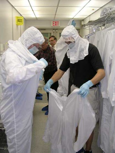
First you need to get dressed in the proper gear to go into the clean room.

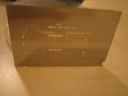
Then you make something like this:

The above device design is just some random one used for instructional purposes. All the features (the text, lines, etc.) imprinted onto the chip are approximately 1.5 micrometers thick. Compare that to the thickness of human hair, which is 80 micrometers on average. The lines you see on the chip can be used to create 1.5 micrometer thick channels so that you can pump fluids through the channels and study flow on the micro-scale. Pretty neat, huh? A similar process to this is used to create those computer chips we all love, though their methods are infinitely more complex of course.
What I find funny is that this is the third time I’ve done this. I’ve made this same exact chip in Cellular/Tissue Engineering Lab, Biomedical Instrumentation Lab, and now Micro/Nanotechnology. Well, people always say repetition is the key to learning.
